
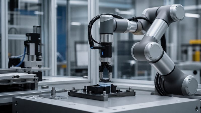
Silicon Valley is home to companies worth trillions of dollars apiece. Apple, Alphabet and Meta all live there. What the region has rarely had is the heavy industrial machinery behind those fortunes. Most chip facilities now operate overseas or in other states, and the local skyline is mostly modest office parks. Applied Materials is trying to change that. On October 12, 2026, the company inaugurated its $5 billion Equipment and Process Innovation and Commercialization (EPIC) Center in Sunnyvale, California. The facility is described as the largest investment in advanced semiconductor R&D in the United States. Inside the EPIC Center The building covers 600,000 square feet. Nearly four acres of that is cleanroom space, the ultra-controlled environment where chip processes are developed and tested. Construction took more than six million hours of labor. The headline goal is speed. Applied Materials aims to shrink the traditional semiconductor development cycle by at least 30%. The mechanism is collaboration. Today, the path from a new chipmaking idea to a working production process tends to move step by step. An equipment maker builds a tool, a chipmaker tests it, researchers stu...
Applied Materials opens $5 billion EPIC Center to speed up AI-era chip development
 54 minutes ago
1
54 minutes ago
1
Related

Starknet launches Shadow Accounts to keep DeFi wallets unlin...
47 minutes ago
0




Popular

Cardano Jumps 11 Percent: What ADA Holders Should Check Befo...
3 weeks ago
106



Bitcoin price tops $77K after BOJ lifts rates to 1.25%
3 weeks ago
73

Bitcoin price rebound faces major test at $83K
3 weeks ago
70



 English (US) ·
 © Clint's Cryto News 2026. All rights are reserved
