
 1 month ago
12
1 month ago
12
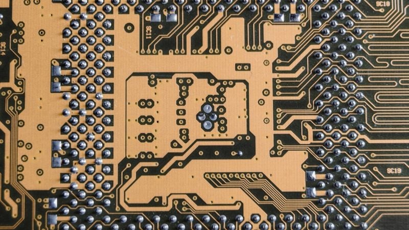
Samsung Electronics is betting that the most expensive machines ever built for chipmaking will give it a decisive edge in the memory wars. The company announced an enhanced strategic partnership with ASML on September 8, 2026, committing to deploy High-NA EUV lithography in mass production of DRAM by 2028. If Samsung hits that target, it would mark the first time any chipmaker has used High-NA EUV technology in the DRAM sector. What High-NA EUV actually means EUV lithography, or extreme ultraviolet lithography, is the technology that prints impossibly tiny circuit patterns onto silicon wafers using light with a wavelength of just 13.5 nanometers. “High-NA” refers to a higher numerical aperture in the lens system — rising from 0.33 to 0.55 — which allows the machine to print even finer patterns with better resolution. The practical benefit for DRAM: fewer manufacturing steps, tighter circuit patterns, and better efficiency. High-NA EUV facilitates single-exposure capabilities, simplifying the previously complex multi-patterning required by older EUV equipment. These machines don’t come cheap. Each High-NA EUV tool costs between $350 million and $400 million. The 12-inch photomask sh...
Related

Best KuCoin alternatives for futures Trading in 2026
15 minutes ago
0

France Crypto Tax Plan Returns to Assembly Debate
20 minutes ago
0

US deploys new drone, communication capabilities in Middle E...
35 minutes ago
0

BitMEX sued for £20 million over Bitcoin losses
35 minutes ago
0
AI investment to hit $600B by 2026, impacting other sectors:...
38 minutes ago
0
Kamala Harris warns the window for AI safeguards is closing,...
43 minutes ago
0

USD stablecoins hold at $303.4 billion while euro tokens rea...
45 minutes ago
0

Epoch AI reports 13-fold annual decline in AI costs as spend...
48 minutes ago
0
Popular

Cardano Jumps 11 Percent: What ADA Holders Should Check Befo...
3 weeks ago
106


Bitcoin price tops $77K after BOJ lifts rates to 1.25%
3 weeks ago
75

Bitcoin price rebound faces major test at $83K
3 weeks ago
70




XRP logo lands on Louisville basketball court
4 weeks ago
63
 English (US) ·
 © Clint's Cryto News 2026. All rights are reserved
