
SK Hynix held a groundbreaking ceremony on August 27 for its first US advanced packaging facility, located at Purdue University’s Research Park in West Lafayette, Indiana. The investment exceeds $4 billion. The facility spans 133.5 acres. And the ambition behind it is simple: make high-bandwidth memory (HBM) chips on American soil to feed the AI industry’s insatiable appetite for faster, denser memory. What SK Hynix is actually building This isn’t a traditional chip fabrication plant. It’s an advanced packaging facility, which means silicon wafers will still be manufactured at SK Hynix’s fabs in South Korea, then shipped to Indiana for the intricate process of stacking and packaging them into finished HBM products. The end result qualifies as “Made in USA,” which matters quite a bit given the current geopolitical climate around semiconductor supply chains. SK Hynix is targeting October 2028 for cleanroom operations to begin. Mass production of HBM4E, the company’s next-generation high-bandwidth memory product, is expected to start in the second half of 2029. HBM is the memory technology that sits inside the AI accelerators powering data centers for companies like Nvidia, Microsoft,...
SK Hynix breaks ground on $4B advanced packaging facility in Indiana
 1 month ago
17
1 month ago
17
Related
Bitcoin, Ether ETFs’ October outflows swell toward $1B
22 minutes ago
0
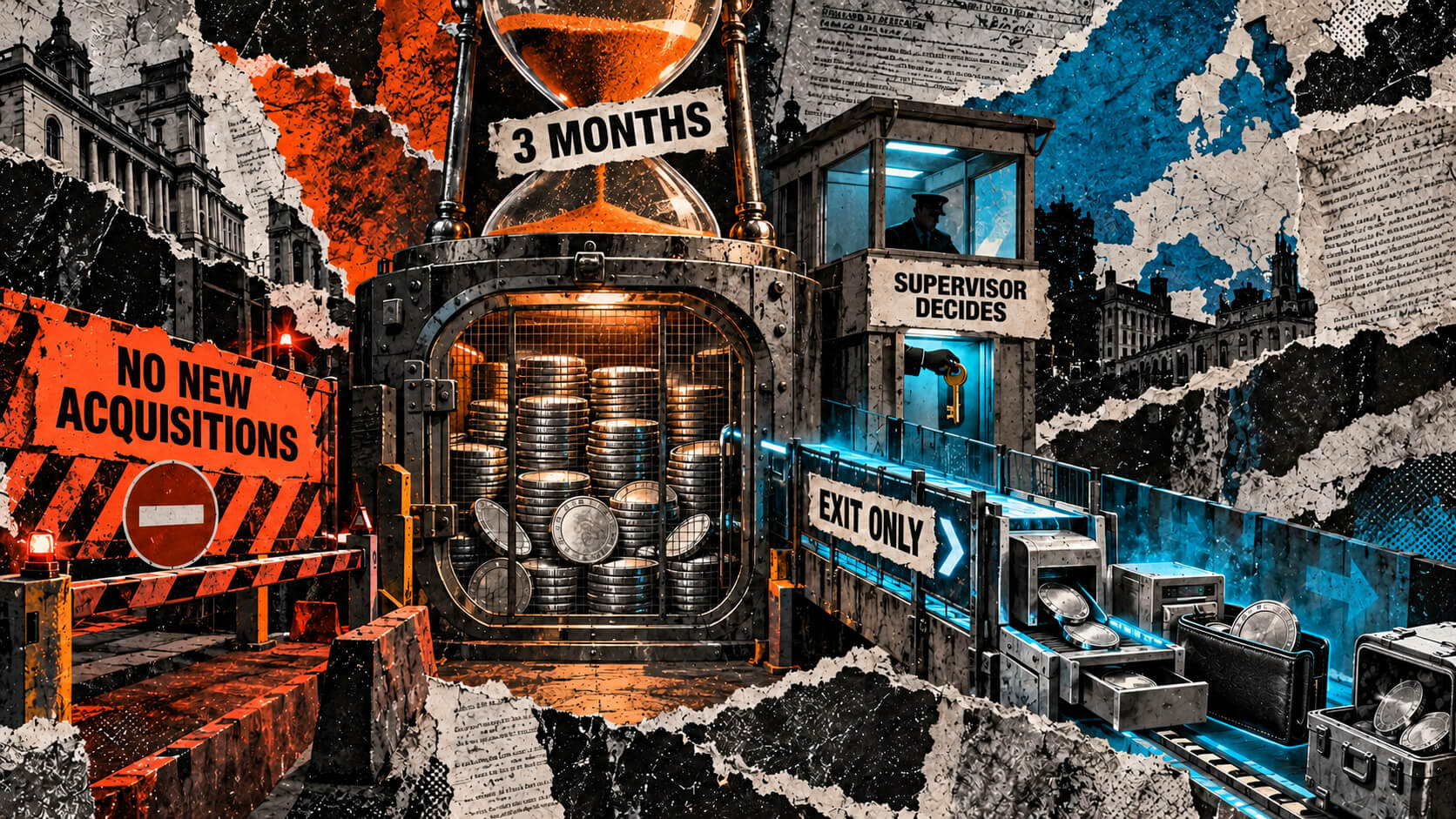
EU regulators target non-compliant stablecoins with a 90-day...
37 minutes ago
0

Crypto firms turn to Anthropic AI to find security flaws
45 minutes ago
0

MARA Holdings moves $81M in BTC, is Bitcoin price at risk?
52 minutes ago
0

As humans leave the loop, verification moves to infrastructu...
57 minutes ago
0


Popular

Cardano Jumps 11 Percent: What ADA Holders Should Check Befo...
2 weeks ago
103



Bitcoin price tops $77K after BOJ lifts rates to 1.25%
3 weeks ago
65

Chainflip loses 736,442 USDT in TRON exploit
3 weeks ago
64

Bitcoin price rebound faces major test at $83K
2 weeks ago
63


 English (US) ·
 © Clint's Cryto News 2026. All rights are reserved
